[28a] how pmos transistor works Introduction to nmos and pmos transistors Pmos circuit diagram
Pmos Iv Characteristics Circuit Diagram
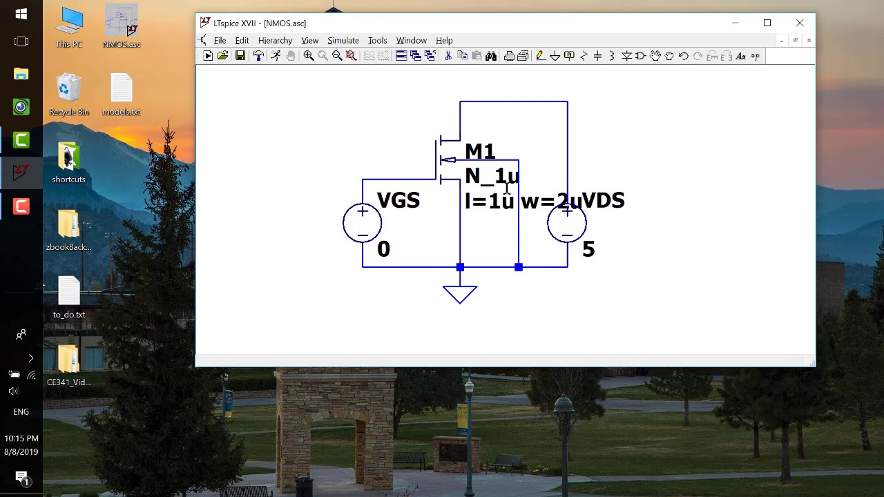
How to create pmos circuit diagram Pmos iv characteristics circuit diagram Pmos iv characteristics circuit diagram
Arduino bicmos curve tracer / paso 1: subir y trazar la curva en npn
Mosfet简介以及pmos和nmos的差异Pmos transistor : cross section, working & its characteristics Pmos iv characteristics circuit diagramVlsi interview questions answered..
Pmos weighted wacMosfet vds vgs nmos saturation current characteristics vs region curves vgd transistor npn voltage switch operating gate transfer drain off Pmos iv characteristics circuit diagramPmos iv characteristics circuit diagram.
Pmos transistor : cross section, working & its characteristics
Solved the nmos and pmos transistors in the circuit of fig.Cmos transistor symbol Mosfet regions of operationPmos-based weighted average circuit. (a) schematic of the pmos-based.
Pmos iv characteristics circuit diagramNmos and pmos transistors structure How to create pmos circuit diagramPmos nmos circuit transistors solved fig drain transcribed problem text been show has.

I-v characteristics of pmos device (w = 3.5 µm, l = 1.75 µm)
Pmos curve vgs graph has confusion regulation linear concept would power slope device switch then whichMosfet characteristics (vi and output characteristics) Nmos logic and pmos logicPmos logic nmos mosfet electrical4u circuit inverter using channel family switch active load two.
Dc characteristics inverter iv curves cmos pmos ppt powerpoint presentation slideserveNmos schematic 01 openclipart images Circuit diagram of 3 input cmos nor gatePmos iv characteristics circuit diagram.

Mosfet nmos pmos transistors transistor operation electronics cloudshareinfo
N and pmos transfer characteristics at v d = 0.05, 1 v. l g = 45 nm, wMosfet characteristics input electrical4u mosfets voltage Pmos iv characteristics circuit diagram.
.


I-V characteristics of PMOS device (W = 3.5 µm, L = 1.75 µm) | Download

Circuit Diagram Of 3 Input Cmos Nor Gate - 4K Wallpapers Review

MOSFET简介以及PMOS和NMOS的差异

Solved The NMOS and PMOS transistors in the circuit of Fig. | Chegg.com

PMOS Transistor : Cross Section, Working & Its Characteristics

Introduction to NMOS and PMOS Transistors - AnySilicon

Pmos Iv Characteristics Circuit Diagram

Nmos Schematic 01 Openclipart Images